
In the intricate cartography of the global economy, the semiconductor industry is undeniably the beating heart. It is the engine of our digital civilization. Yet, the seismic events of recent years-from unprecedented chip shortages to historic logistical disruptions-have taught us a sobering lesson: this vital supply chain, the intricate web that powers our world, is far more fragile than we ever imagined. The failure of a single, seemingly minor link can trigger a chain reaction with profound and far-reaching consequences.
Within this complex and vulnerable chain, there exists a critical, often-overlooked component: semiconductor packaging and handling materials.
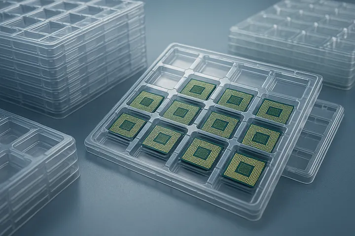
The wafers, dies, and integrated circuits at the heart of our technology are miracles of creation, but they are also incredibly fragile. Their journey through hundreds of manufacturing steps, their storage, and their global transport all depend on a suite of highly specialized packaging materials. These are not mere “boxes” or “trays.” They are high-precision engineering carriers, meticulously designed to interface with billion-dollar automated systems and to protect their priceless cargo from the triple threats of physical shock, electrostatic discharge (ESD), and microscopic contamination.
When the supply of these critical carriers is delayed or disrupted, the entire output of a multi-billion-dollar fabrication plant can grind to a halt. The financial losses are astronomical.
Traditionally, these packaging materials have been the domain of large, overseas manufacturers who rely on standardization and massive production scales. But in the face of today’s industry trends-smaller, more diverse production batches, rapid R&D cycles, and endemic supply chain instability-the market desperately needs a more agile and flexible solution.
This is precisely the role that IDMockup & Precision Mold has been fulfilling for years. As a hidden champion within Taiwan’s world-leading semiconductor ecosystem, we provide a core strategic value. We are not just a component manufacturer; we are your strategic partner in overcoming the critical packaging challenges of the modern era.
The High-Stakes World of Semiconductor Packaging: Why It’s So Demanding
Before exploring the solutions, it is crucial to understand why semiconductor packaging is one of the most demanding applications for precision manufacturing. The requirements are absolute, and the margin for error is zero.
The Purity Mandate: The environment inside a semiconductor process chamber is often a high vacuum. A packaging material like a process carrier must be made from materials with low outgassing properties. This means they do not release volatile molecules under vacuum or heat, as even a few stray molecules could contaminate the wafer surface and ruin the delicate lithography process. The material must also exhibit extremely low particle shedding to prevent microscopic dust from landing on the wafer.
The Ever-Present ESD Threat: Modern microchips have circuit features so small that a single, invisible spark of static electricity can be catastrophic, puncturing a gate oxide and destroying the component. All handling materials must therefore be made from materials with specific, tightly controlled static-dissipative (ESD) properties to safely bleed off any static charge.
The Automation Imperative: A modern semiconductor fab is a ballet of high-speed robotics. Wafers and trays are moved by automated material handling systems (AMHS), and chips are manipulated by pick-and-place machines operating at incredible speeds. The packaging-be it a wafer frame or a JEDEC tray-is a piece of tooling that must interface with this machinery with absolute precision. A dimensional error of even 0.1mm on a tray can cause a robotic handler to jam, leading to a costly line-down event and potentially damaging a whole batch of valuable chips.
These three mandates-purity, ESD protection, and automation-grade precision-form a high barrier to entry that only the most specialized manufacturers can clear.
Challenge #1: The R&D Agility Gap and the Tyranny of Lead Times
The pace of semiconductor innovation is relentless. An R&D team may develop a new, non-standard chip package, a specialized sensor with a unique footprint, or a thinner wafer that requires a new type of support frame. A critical and immediate problem arises: there is no off-the-shelf packaging available to handle, test, and validate these new creations.
The traditional path to solving this is fraught with delays. The team would need to contact a large, overseas mass-producer of packaging, negotiate a custom tool, likely face a high Minimum Order Quantity (MOQ), and then wait. The process of quoting, tool fabrication, first article inspection, and shipping can often stretch for two to four months.
In the hyper-competitive race to market, this multi-month delay is not just an inconvenience; it is a critical competitive disadvantage.
IDMockup’s Solution: Localized, Rapid, On-Demand Customization
This is where our deep expertise in high-precision CNC machining becomes a strategic weapon for our clients. We have transformed this “months-long” problem into a solution delivered in a matter of days.
The process is one of pure agility. The moment a client provides us with a 3D design file (e.g., a STEP file), our engineering team conducts a rapid manufacturability review, and our CAM programmers begin developing the optimal toolpaths. We specialize in machining the exact high-performance engineering plastics specified by the semiconductor industry, such as PEEK, Torlon®, and Vespel®, chosen for their unique combination of anti-static properties, high-temperature stability, and chemical resistance.
Our state-of-the-art 5-axis CNC machines, equipped with tooling specifically for these advanced polymers, can then begin production immediately. We can deliver the first, the tenth, or the fiftieth piece of a completely custom-designed wafer frame, process carrier, or chip tray in just a few days. This allows our clients’ R&D teams to proceed with testing and validation almost instantaneously, dramatically accelerating their development cycles and helping them win that precious race to market.
Challenge #2: The Supply Chain Fracture and the Peril of Production Stoppages
A container ship delayed by a storm, a geopolitical conflict that closes a border, a sudden spike in demand that overwhelms a supplier-these are the new realities of the global supply chain. For a fab manager, the nightmare scenario is a production line worth billions of dollars sitting idle because a shipment of a seemingly simple component, like a standard IC shipping tray, is stuck in transit. The cost of a line-down event, even for a few hours, can run into the millions of dollars.
IDMockup’s Solution: Localized Emergency and Bridge Production
In this scenario, IDMockup acts as a form of “supply chain insurance.” We are our clients’ local Emergency Response Unit. When a critical gap appears in their conventional supply chain, we have the capability to react with incredible speed.
Rapid Replication: If a standard part is needed, a client can provide us with a sample. Using our advanced CMM (Coordinate Measuring Machine) and 3D scanning technology, we can quickly and accurately reverse-engineer the component to create a precise digital model.
Bridge Manufacturing: We can then immediately activate our production capacity to manufacture a small-to-medium batch of these critical packaging components. This “bridge” production run is designed to supply our client’s immediate needs, keeping their production lines running while they await the arrival of their larger, overseas order.
Guaranteed Compatibility: The key to making this work is our unwavering commitment to precision. We manufacture these emergency parts to the exact same, if not tighter, tolerances as the originals, holding dimensions to ±0.01mm. This guarantees that our components are a 100% “drop-in” replacement, perfectly compatible with their existing high-speed automated equipment. This capability minimizes disruption and provides an unprecedented level of operational resilience.
Challenge #3: The Unwavering Standard of Materials and Precision
As established, semiconductor packaging is not a commodity. It is a high-precision, technically demanding product. This is not a field where “good enough” is acceptable.
IDMockup’s Solution: A Foundation of Deep Expertise
This is the very core of our competitive advantage. We have not simply invested in advanced machinery; we have invested decades in building a deep, institutional knowledge of semiconductor-grade materials, the unique craft of machining them, and the specific needs of the industry itself.
Our engineering team is intimately familiar with the processing characteristics of the most advanced polymers. We understand the precise feeds, speeds, and cutting tools required to machine a material like PEEK without introducing stress or subsurface cracking. We know how to achieve a flawless, burr-free surface finish to prevent particle shedding. We understand the design considerations for ensuring ESD safety and automation compatibility.
Every component we deliver is a representation of our commitment to precision and quality. It is this foundational expertise that enables us to so effectively solve the challenges of R&D agility and supply chain disruption. We don’t just make parts; we engineer solutions built upon a bedrock of deep industry knowledge.
Conclusion: Building a More Resilient Semiconductor Supply Chain with Localized Agility
In an era of increasing global uncertainty, the old strategy of relying on long, rigid, single-source supply chains has been exposed as a high-risk gamble. For Taiwan’s world-leading semiconductor industry, and indeed for the global industry as a whole, building a more resilient, agile, and responsive local supply chain is a key strategic imperative for future success.
IDMockup & Precision Mold provides precisely this solution. With our rapid customization capabilities, our flexibility to respond to emergencies, and our unwavering commitment to quality, we fill the critical gaps that traditional, large-scale manufacturing models cannot address. We provide semiconductor clients with a more flexible, more reliable, and ultimately, a more secure option when facing the challenges of new product development and supply chain volatility.
Do not let a small, seemingly simple packaging component become the bottleneck that constrains your innovation and growth. Partner with a local precision manufacturer that understands the stakes. Let IDMockup become your strategic partner in building a safer, stronger, and more resilient lifeline for your semiconductor operations.
Interested in learning more about our related manufacturing capabilities? Explore our CNC & EDM Machining, 3D Printing, Rapid Tooling & Injection Molding, Vacuum Casting (Soft Tooling), Reaction Injection Molding (RIM), and Metal Die Casting pages.