
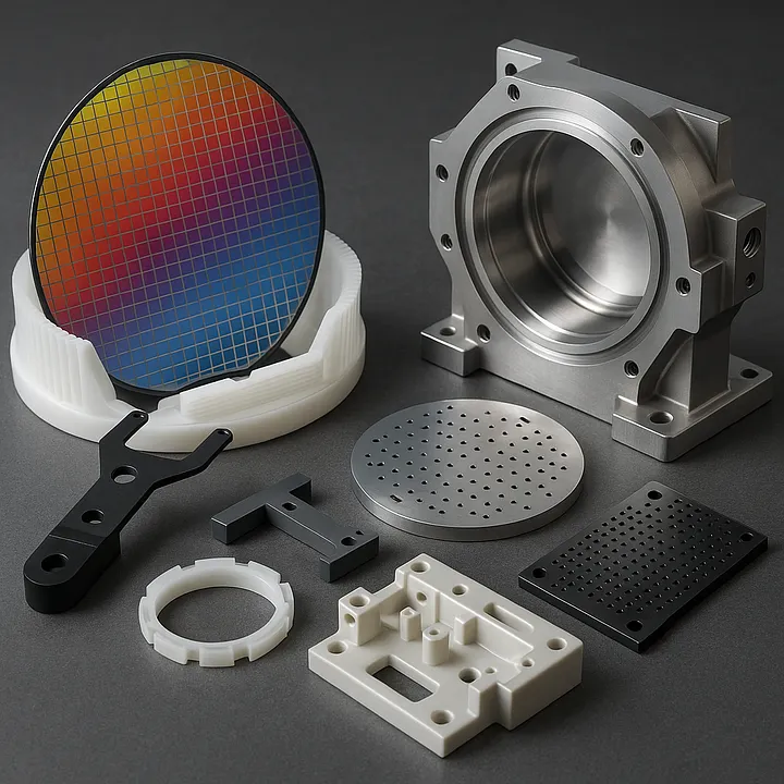
The semiconductor is the beating heart of modern digital civilization. Every facet of our lives-from the smartphone in your hand and the AI servers in the cloud to the computational core of an autonomous vehicle-originates from a sliver of silicon, a chip forged in an environment of absolute cleanliness and almost unimaginable precision. The cutting-edge equipment that creates these miracles of modern science is, itself, a technical marvel, an intricate assembly of countless ultra-high-precision components.
In the uncompromising world of the semiconductor industry, the standards are absolute. Every component’s dimensional tolerance, its material properties, and its surface purity can directly impact the final chip’s yield and performance. A deviation measured in microns can be the difference between a multi-million-dollar success and a catastrophic failure. This is a world that does not permit error. Consequently, when equipment developers and manufacturers select a partner for their critical components, the standards for qualification far exceed those of any other industrial sector.
For years, IDMockup & Precision Mold has proudly served as such a trusted and critical partner in this demanding ecosystem. We are more than just model makers; we are a specialized, high-capability manufacturing partner providing the core precision components that form the backbone of the semiconductor equipment supply chain. Leveraging a deep, institutional understanding of specialty materials and a mastery of micron-level machining, we provide the solid, reliable foundation for every stage of the semiconductor manufacturing process.
Today, we invite you into the world of IDMockup’s precision workshop to explore the landscape of critical products we have the proven expertise to build for the semiconductor industry.
1. The Guardians of the Wafer: Precision Handling, Transport, and Process Carriers
The silicon wafer is the most fundamental and precious material in semiconductor manufacturing. A single 300mm wafer can hold hundreds of complex processors, representing an immense value. Throughout its journey of hundreds of process steps, its handling, fixation, and transport must be conducted under conditions of absolute sterility, with zero risk of contamination, electrostatic discharge (ESD), or physical scratches. Any minuscule flaw introduced by a handling component can result in the scrapping of the entire wafer.
The Products We Engineer:
- Wafer Handling End-Effectors: These are the highly specialized “hands” that attach to the end of robotic arms to gently yet securely grip and transport wafers. They are custom-designed for different wafer sizes and applications, from atmospheric to vacuum environments.
- Wafer Frames: During critical processes like wafer backgrinding and dicing, the now incredibly thin and fragile wafer must be mounted on a rigid frame for support and stability. We manufacture these frames to exact specifications.
- Custom Process Jigs & Fixtures: Every piece of semiconductor equipment requires custom tooling to precisely locate, hold, and support wafers during a specific process. We collaborate with equipment engineers to design and manufacture these highly specialized, application-specific jigs and fixtures.
- Critical Components for Cassettes and FOUPs: We manufacture key internal components for the cassettes and Front-Opening Unified Pods (FOUPs) that are used to store and transport wafers between process tools.
IDMockup’s Manufacturing Expertise:
We understand that for these components, the choice of material and the quality of the machining are not just details-they are everything. Our expertise is built upon:
Mastery of Advanced Engineering Plastics: We specialize in machining a portfolio of elite polymers specifically chosen for their performance in ultra-clean environments. Materials like PEEK (Polyetheretherketone), Torlon® (PAI), and Vespel® (PI) are our daily business. We understand their unique properties:
- Anti-Static (ESD): To prevent electrostatic discharge from damaging the delicate circuits on the wafer.
- High-Temperature Resistance: To withstand thermal processes without deforming or degrading.
- Chemical Resistance: To endure exposure to the aggressive chemicals used in cleaning and etching processes.
- Low Outgassing: A critical property for use in high-vacuum process chambers, ensuring no molecules are released from the plastic that could contaminate the wafer surface.
- High Purity & Low Particle Shedding: To ensure the component itself does not become a source of contamination.
Ultra-Precision 5-Axis CNC Machining: Using our state-of-the-art 5-axis CNC centers, we machine these advanced plastics to achieve exceptionally smooth, non-abrasive surfaces. We hold dimensional tolerances to within ±0.01mm (10 microns), a level of precision that guarantees a perfect interface with both the delicate wafer and the automated equipment. This is how we perfectly guard every precious wafer.
2. The Crucible of Creation: Core Components for Process Equipment
In the “front-end-of-line” (FEOL) manufacturing process, a wafer undergoes a trial by fire. It is subjected to the extreme environments of Chemical Vapor Deposition (CVD), Physical Vapor Deposition (PVD), Plasma Etching, and Chemical-Mechanical Planarization (CMP). The components inside these process chambers must be incredibly robust, capable of withstanding high temperatures, high vacuum, constant plasma bombardment, and long-term exposure to corrosive gases.
The Products We Engineer:
- CMP Retaining Rings: These are critical, high-wear components used in the CMP process. The ring holds the wafer in place on the polishing head and plays a crucial role in controlling the slurry flow, which is essential for achieving the nanometer-level surface planarity required for modern chips.
- Gas Showerheads: In deposition and etch chambers, these complex components are used to uniformly distribute process gases over the wafer surface. They contain intricate patterns of precisely drilled micro-holes to ensure process uniformity.
- Chamber Liners & Insulators: These components protect the main process chamber from the harsh conditions within, and they provide electrical and thermal insulation.
- Plasma Etch Components: A variety of parts designed to operate within, and withstand the erosive effects of, a high-energy plasma environment.
IDMockup’s Manufacturing Expertise:
Manufacturing these components is a true test of a company’s technical depth, and it is where our capabilities truly shine.
Machining the “Unmachinable”: Beyond advanced plastics, we have cultivated a deep expertise in machining hard and brittle materials that are essential for the semiconductor industry. This includes:
- Machinable Ceramics (like Macor®): Offering excellent thermal and electrical insulation.
- Quartz and Sapphire: For components requiring optical transparency or extreme plasma resistance. Our engineering and machining teams understand the unique challenges of these materials-their tendency to chip, their abrasive nature-and have developed specialized tooling, fixtures, and machining strategies to overcome them.
Realizing Complex Geometries: We possess the technology and the knowledge to create the complex internal features these parts demand, such as intricate fluidic channels, arrays of micro-holes with high aspect ratios, and surfaces machined to an optical-grade flatness. This expertise ensures the stability, reliability, and long service life of these critical components in the most extreme process environments.
3. The Arbiters of Quality: Components for Back-End Assembly, Test & Inspection
Once the wafer fabrication is complete, the process moves to the “back-end-of-line” (BEOL). Here, the wafer is diced into individual chips, which are then tested, sorted, and packaged. This stage is a world of high-speed, high-precision automation.
The Products We Engineer:
- Enclosures and Chassis for Test & Inspection Equipment: We provide high-quality, finished aluminum housings, panels, and structural frames for a wide range of back-end equipment, including Automated Test Equipment (ATE), probe card testers, and Automated Optical Inspection (AOI) systems.
- Chip Test Sockets & Nests: These are highly precise, custom-machined nests, often made from specialized static-dissipative plastics, that hold a single chip in a precise location for functional electrical testing.
- Components for Sorters & Pick-and-Place Machines: The arms, vacuum nozzles, and track components for the high-speed robotic systems that sort and handle individual dies.
IDMockup’s Manufacturing Expertise:
This domain showcases our capability as an integrated, one-stop manufacturing partner. We demonstrate a seamless fusion of our different areas of expertise:
Dual-Material Capability: We have the ability to produce both the internal, non-conductive engineering plastic components (like the test sockets) and the external, robust, and thermally conductive aluminum alloy enclosures and chassis for the equipment itself.
Complete Finishing Solutions: For the equipment housings, we provide a full suite of finishing services, including precision CNC machining, anodizing for durability and aesthetics, and laser engraving or silk-screening for professional branding and labeling.
This ability to deliver a complete solution-from the internal functional parts to the fully finished external structure-provides immense value to our clients, simplifying their supply chain and ensuring perfect integration between all components.
Conclusion: With Micron-Level Precision, We Build the Industry’s Foundation
From the first delicate handling of a new wafer, to the fiery crucible of its creation, and onto the final judgment of its quality, every single step in the semiconductor industry is built upon an unyielding foundation of precision.
At IDMockup & Precision Mold, we are proud to be a deeply integrated part of this foundational layer. Our contribution is forged from our mastery of specialty materials, our relentless dedication to precision machining, and our profound understanding of our clients’ unique and demanding requirements. The components we manufacture may be just a small part of a massive, complex piece of equipment, but we understand that it is the flawless synergy of thousands of such perfect parts that enables the construction of the entire, magnificent edifice of the semiconductor industry.
If your team is developing the next generation of semiconductor equipment, or if you are in need of a higher-quality, more reliable source for your critical process components, IDMockup & Precision Mold stands ready. We are prepared to bring our decades of accumulated professional experience to your project, serving as your most trusted manufacturing partner.
Interested in learning more about our related manufacturing capabilities? Explore our CNC & EDM Machining, 3D Printing, Rapid Tooling & Injection Molding, Vacuum Casting (Soft Tooling), Reaction Injection Molding (RIM), and Metal Die Casting pages.