
Precision Parts for the
Semiconductor Industry
CNC precision machining, 3D printing, and rapid prototyping for semiconductor manufacturing equipment, IC packaging fixtures, wafer handling systems, and cleanroom-compatible tooling.
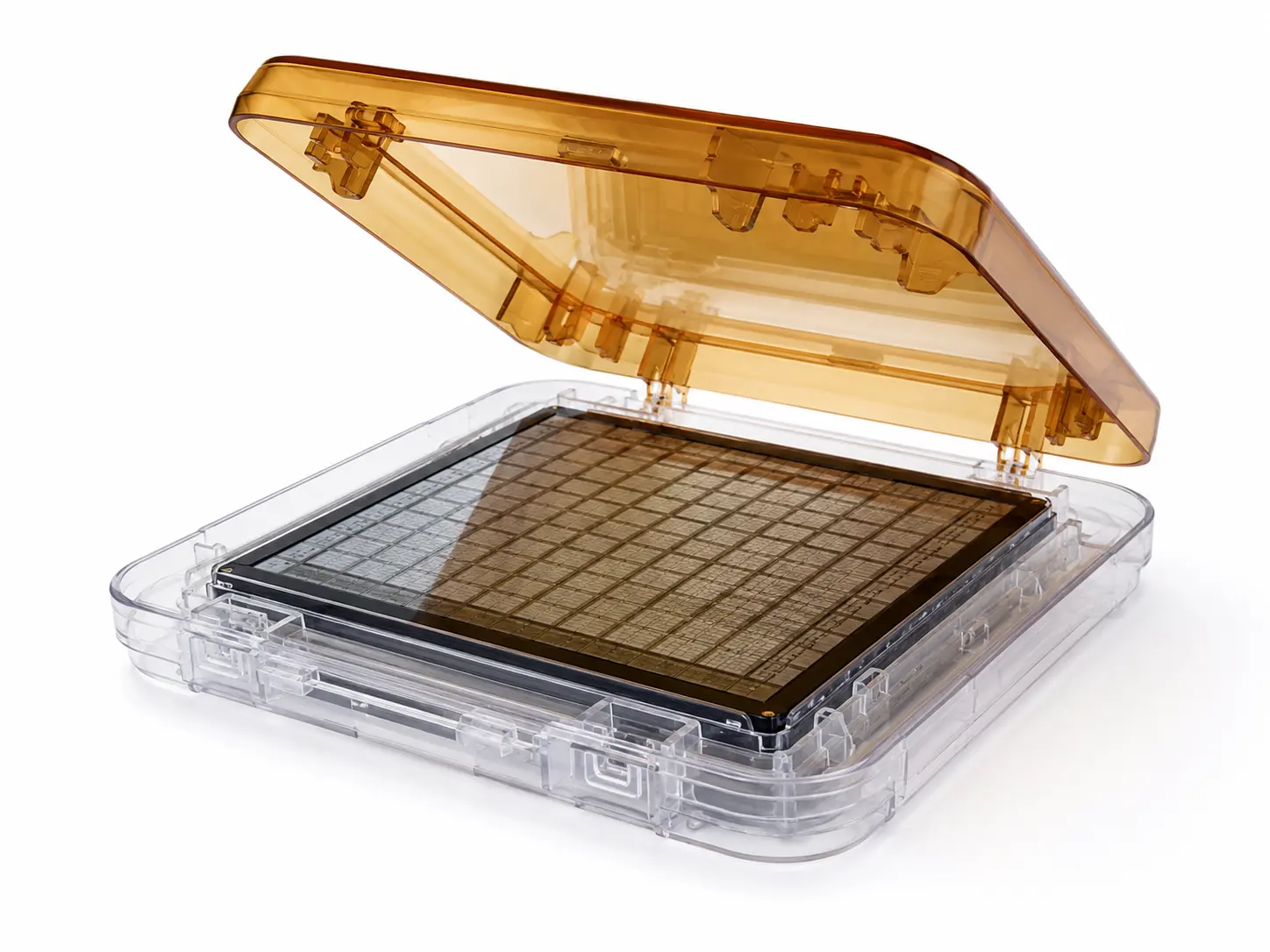
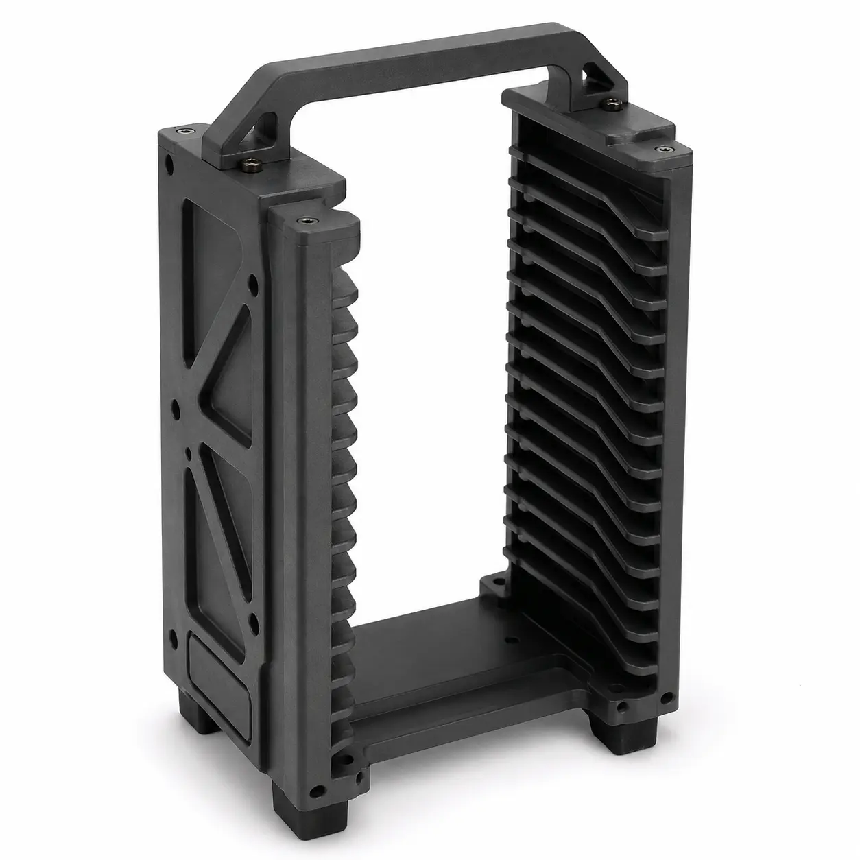
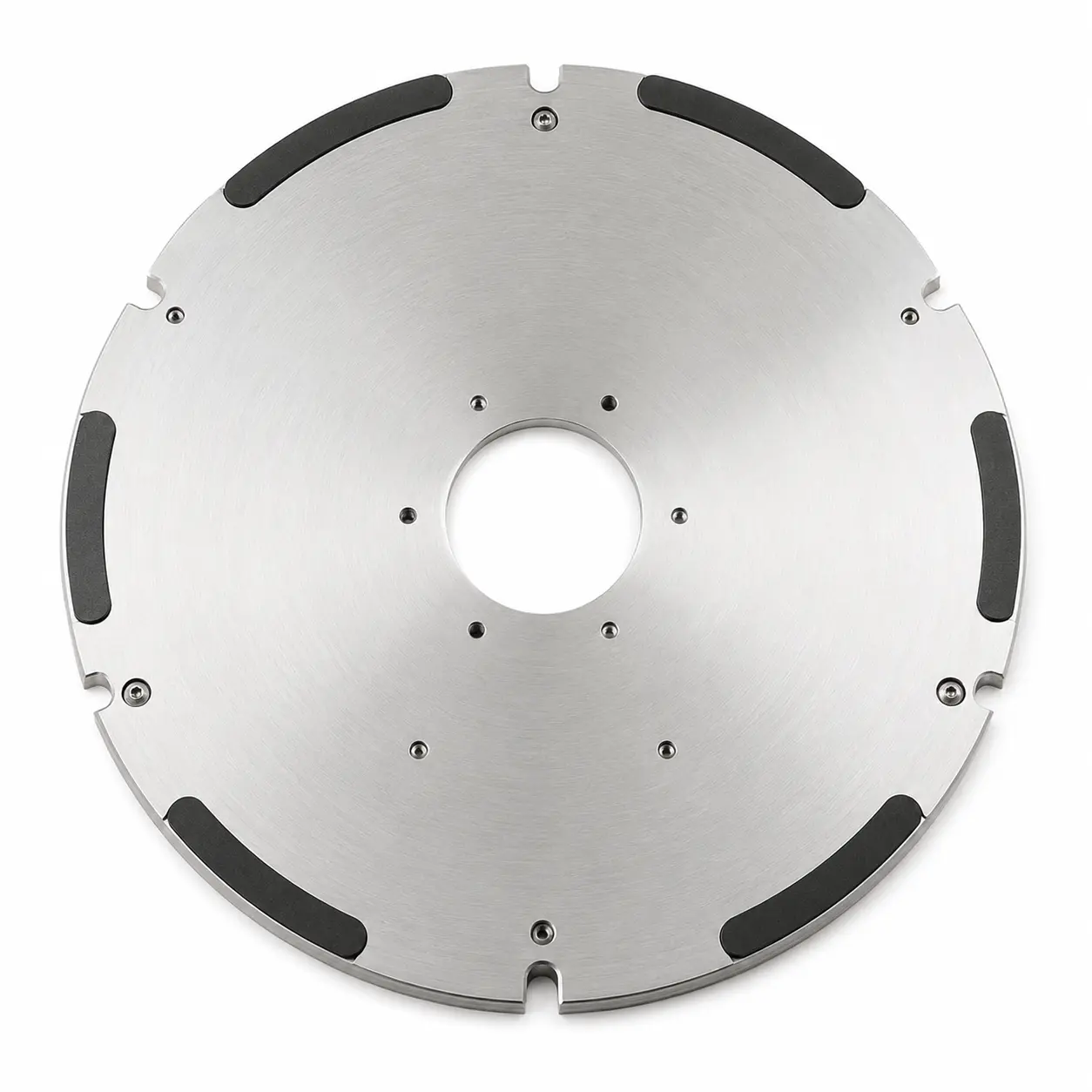
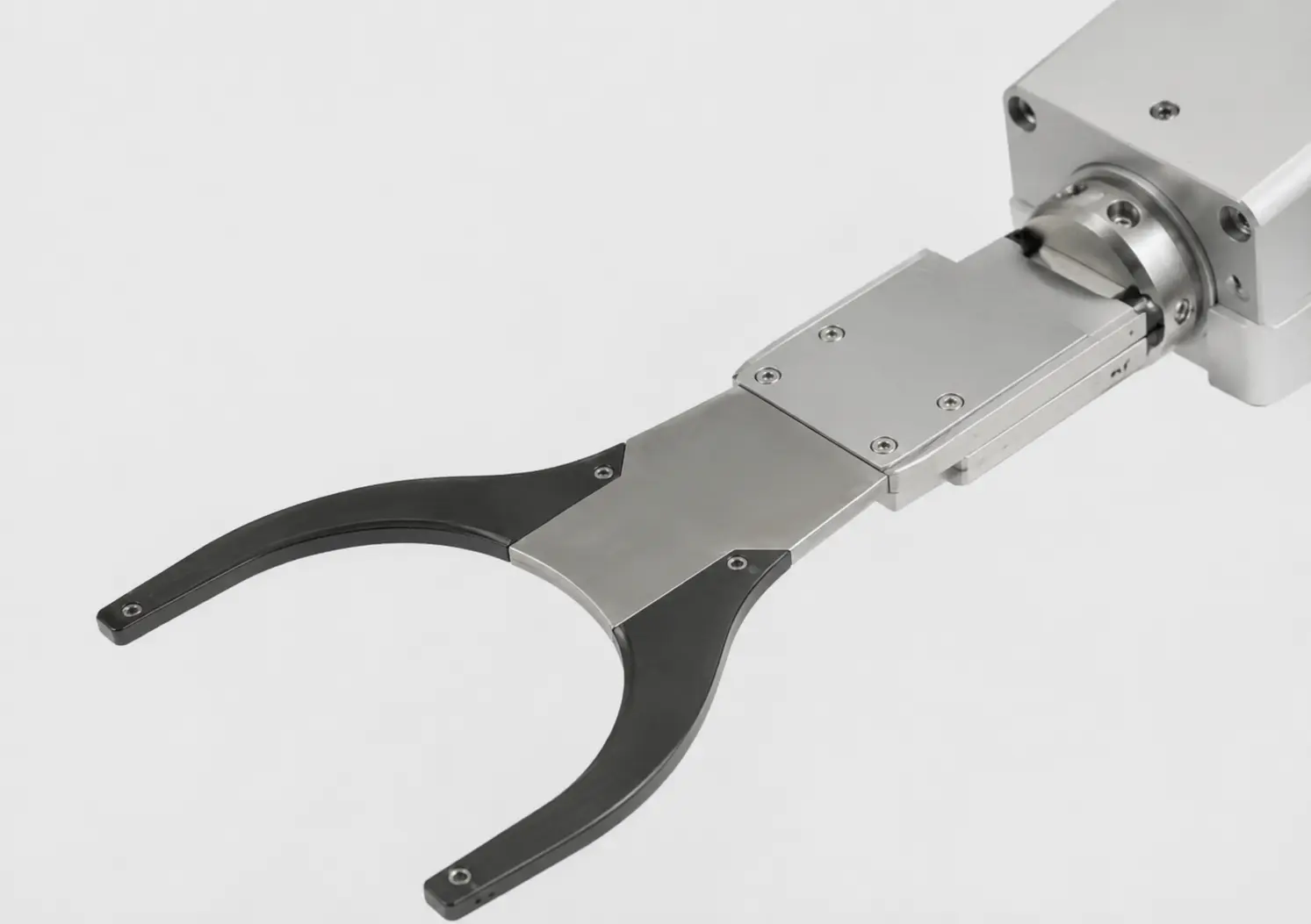
Semiconductor Parts & Fixtures in Action
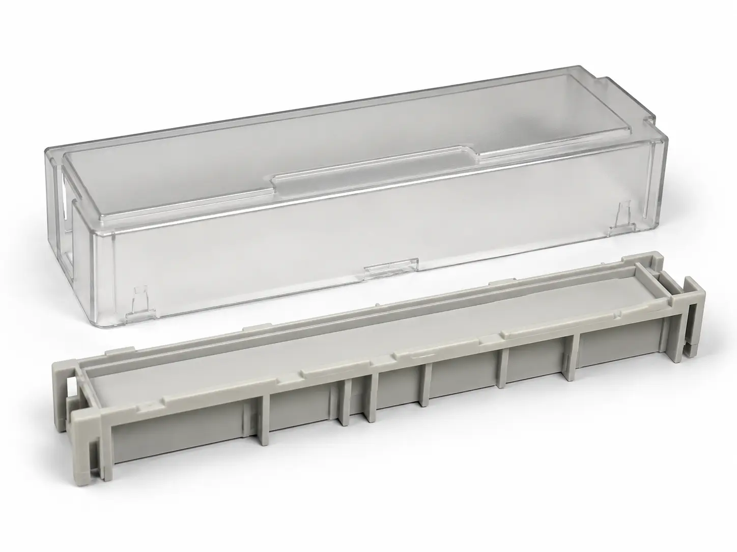
Why Semiconductor Teams Rely on Precision Prototyping
Equipment Design Validation
Verify CNC-machined chamber components, robot arm end-effectors, and wafer carrier geometries against drawing tolerances before committing to expensive production runs.
Fixture & Jig Prototyping
Rapidly prototype wafer handling fixtures, burn-in boards, IC socket frames, and test jigs — reducing equipment qualification timelines by weeks.
Thermal & Mechanical Testing
Validate thermal uniformity, mechanical stress tolerance, and vacuum integrity of chamber components under simulated process conditions.
IC Packaging Verification
Test IC packaging design, thermal management paths, and electrical connection stability with precision metal and plastic mockups before production tooling.
Ultra-Tight Tolerance Parts
Semiconductor equipment demands tolerances at ±0.01mm or tighter. Our 5-axis CNC centers and EDM deliver the dimensional accuracy your processes require.
Qualification & Audit Samples
Supply dimensionally verified samples for equipment qualification, supplier audits, and OEM approval processes in semiconductor fab environments.
Semiconductor Equipment Applications
From front-end of line (FEOL) lithography equipment to back-end IC packaging — we machine, print, and fabricate the parts that keep fabs running.
Wafer Handling & Transport
End-effectors, wafer carriers, FOUP door mechanisms, and robot arm components — precision machined in AL6061, SUS304, or PEEK for cleanroom compatibility.
IC Packaging & Testing
IC socket frames, burn-in test boards, BGA fixtures, and packaging molds — prototyped with ±0.01mm tolerance to validate design before hard tooling.
Lithography Equipment Parts
Reticle stage components, lens barrel brackets, and EUV/ArF exposure unit frames — machined from aluminium alloy or titanium to sub-micron geometric accuracy.
CVD / PVD Deposition Equipment
Susceptors, shower heads, gas distribution plates, and reactor chamber liners — manufactured in AL6061, SiC, or quartz-compatible materials for high-temperature process stability.
CMP & Planarization Tools
Polishing head components, slurry delivery rings, retaining rings, and conditioning disc holders — manufactured to precise concentricity and flatness requirements.
Backend & Assembly Equipment
Die bonder collets, wire bond capillaries, flip-chip fixtures, and dicing tape frames — rapid prototyped and delivered in days for assembly process development.
End-to-End Semiconductor Manufacturing Services
CNC Precision Machining
3 / 5-axis milling & turning to ±0.05mm. AL6061, SUS304, ceramic, and PEEK machined for semiconductor process equipment.
Learn more →EDM Wire & Sinker Cutting
Wire EDM and die-sinking for hard metal parts with complex profiles — burr-free, tight-tolerance semiconductor tooling.
Learn more →3D Printing (SLA/SLS/FDM)
Rapid fixture prototyping in engineering resins and nylon. Fast validation of fit, form, and function before CNC commits.
Learn more →Vacuum Casting
Silicone tooling for 5–50 unit prototype runs of IC packaging fixtures, test adaptors, and handling trays.
Learn more →Reaction Injection Molding
Mid-volume RIM production of semiconductor equipment enclosures and carrier trays — 50 to 5,000 units.
Learn more →Aluminum Die Casting
High-pressure die casting for heat sinks, equipment frames, and structural semiconductor tooling components.
Learn more →Rapid Tooling & Injection
Bridge tooling for pre-production validation runs — weeks faster than conventional hard tooling investment.
Learn more →3D Scanning & Reverse Eng.
High-accuracy scanning of legacy semiconductor tooling — regenerate worn or obsolete equipment parts digitally.
Learn more →Cleanroom-Compatible Materials & Tolerances
Semiconductor processes demand materials with extreme chemical resistance, thermal stability, and zero contamination. We stock and machine the exact grades your fab requires.
Parts destined for cleanroom environments are deburred, ultrasonically cleaned, and packaged in ISO-grade cleanroom bags. Material certifications and inspection reports available upon request.
From Drawing to Delivery — 5 Steps
Inquiry
Submit 3D drawings or sample. Receive a detailed quotation within 24 hours.
DFM Review
Engineers analyse tolerances, material choices, and surface specs before machining.
Precision Machining
CNC, EDM, or 3D printing begins with real-time progress updates.
Surface Treatment
Anodizing, passivation, or electropolishing applied to specification.
CMM QC & Delivery
Coordinate measuring machine inspection. Cleanroom-packaged and shipped worldwide.
Trusted by Global Electronics & Semiconductor Leaders







Ready to Machine Your Next
Semiconductor Equipment Part?
Send us your 3D drawings or technical specifications. Our semiconductor manufacturing team responds with a detailed quote — material selection, tolerance confirmation, and lead time — within 24 hours.
Semiconductor Manufacturing Equipment Parts & Prototyping — IDMockup
IDMockup is a precision manufacturing company specializing in semiconductor manufacturing equipment parts, fixtures, and prototypes. Headquartered in Taiwan with factories in Dongguan, Kunshan, and Thailand, we supply CNC-machined components, EDM-cut tooling, and 3D-printed prototypes to semiconductor equipment OEMs and fab operators worldwide. Our semiconductor equipment parts capabilities cover wafer handling end-effectors, IC packaging test fixtures, CVD/PVD chamber components, CMP tooling, lithography equipment brackets, and backend assembly jigs. Materials include AL6061, SUS304/316L, Ti-6Al-4V, PEEK, PTFE, SiC, and ceramics — all cleanroom-compatible and supplied with full material certifications. Trusted by Dell, Chicony, ECS, Lite-On, Gigabyte, Foxconn, and Wistron, our semiconductor precision machining services support equipment qualification, pilot production, and on-demand spare part supply across the global semiconductor industry.